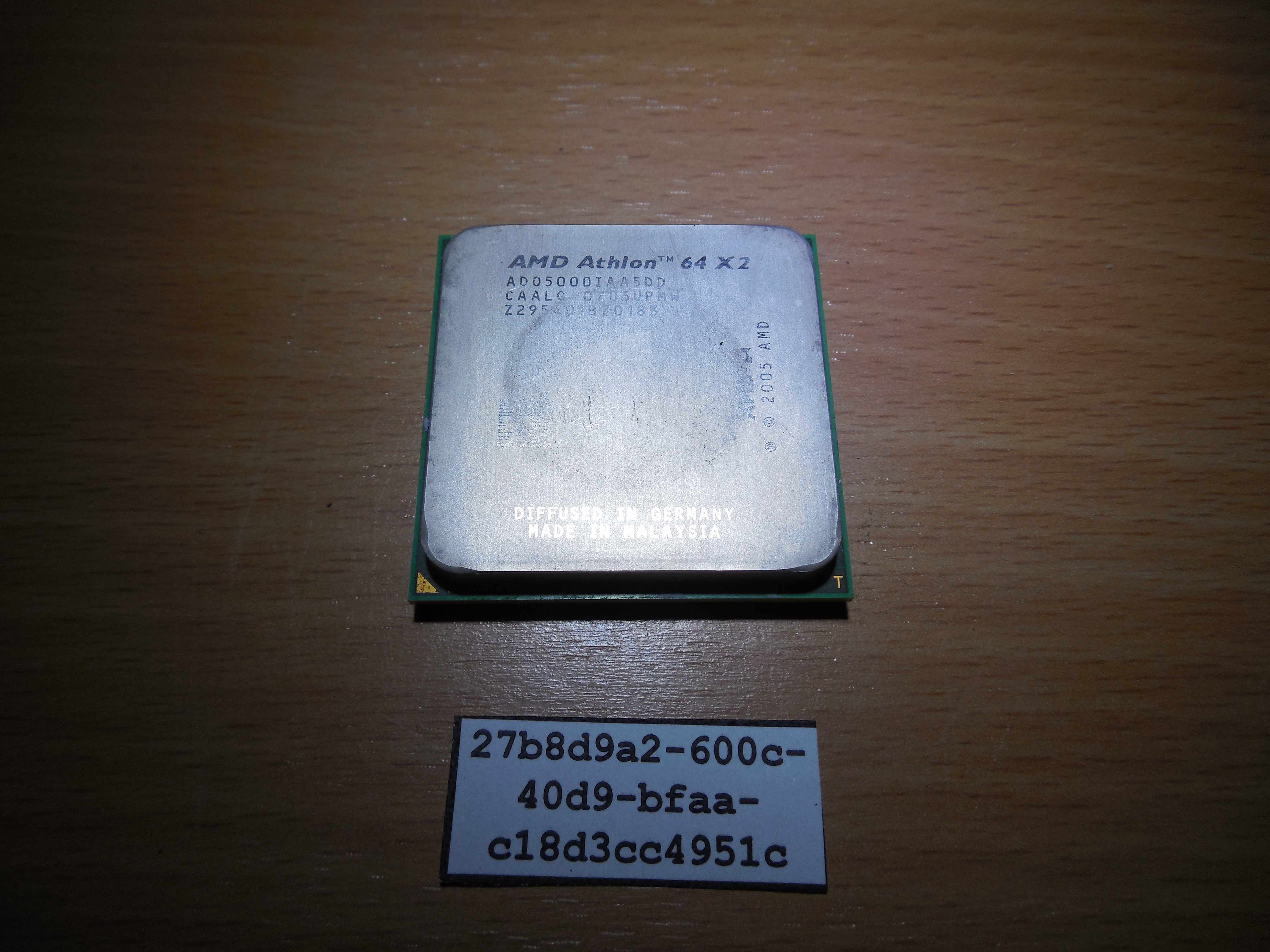

AMD Athlon™ 64 X2
AD05000IAA5DD
CAALG 0705UPMW
Z295401B70183
AMD
(m) (C) 2005 AMD
DIFFUSED IN GERMANY
MADE IN MALAYSIA
Category Archives: Процессоры
Процессор Intel Celeron SL7TW Socket LGA775 (Intel Celeron D 336)

SL7TW specifications
| General information | |
| Type | CPU / Microprocessor |
| Family | Intel Celeron D |
| Processor number ? | 336 |
| Part number | JM80547RE072CN BX80547RE2800CN |
| Frequency (GHz) ? | 2.8 |
| Bus speed (MHz) ? | 533 |
| Clock multiplier ? | 21 |
| Package type | 775-land FC-LGA4 |
| Socket type | Socket 775 (LGA775) |
| Architecture / Microarchitecture / Other | |
| CPUID | 0F41h |
| Core stepping | E0 |
| Manufacturing technology (micron) | 0.09 |
| L2 cache size (KB) ? | 256 |
| Features | EM64T technology ? |
| Core voltage (V) ? | 1.25 — 1.4 |
| Case temperature (°C) ? | 67.7 |
| Package revision | 01 |
| Notes on sSpec SL7TW | |
|
|
Процессор AMD Athlon-64 ADA3500DAA4BW Socket 939 2200Mhz 3500+ (512/1000/1,4v) Venice(ADA3500DAA4BW)
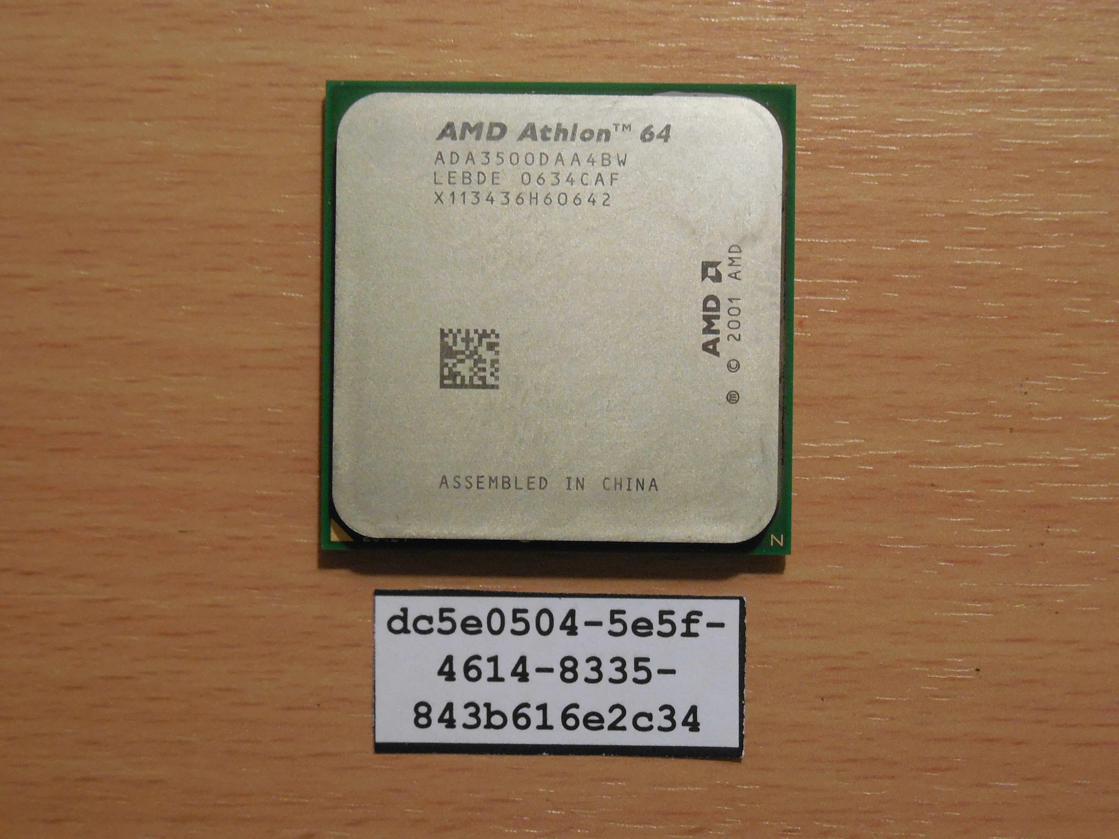
Процессор AMD Athlon 64 ADA3500DAA4BW Socket 939 3500+ (ADA3500BWBOX)


AMD Athlon 64 3500+ specifications
| General information | |
| Type | CPU / Microprocessor |
| Market segment | Desktop |
| Family | AMD Athlon 64 |
| Model number ? | 3500+ |
| CPU part numbers |
|
| Stepping codes | ABBWE CAB2E CACAE LBBWE LEBBE LEBCE LEBDE NBBWE |
| Frequency ? | 3500+ (rated) 2200 MHz (real) |
| Bus speed ? | One 1000 MHz 16-bit HyperTransport link (2GT/s) |
| Clock multiplier ? | 11 |
| Package | 939-pin lidded organic microPGA 1.57″ x 1.57″ (4 cm x 4 cm) |
| AMD Package number | 28727 |
| Socket | Socket 939 |
| Architecture / Microarchitecture | |
| Microarchitecture | K8 |
| Processor core ? | Venice |
| Core stepping ? | DH-E6 |
| CPUID | 20FF2 |
| Manufacturing process | 0.09 micron silicon-on-insulator (SOI) technology |
| Data width | 64 bit |
| The number of cores | 1 |
| The number of threads | 1 |
| Floating Point Unit | Integrated |
| Level 1 cache size ? | 64 KB 2-way set associative instruction cache 64 KB 2-way set associative data cache |
| Level 2 cache size ? | 512 KB exclusive 16-way set associative cache |
| Physical memory | 1 TB |
| Virtual memory | 256 TB |
| Multiprocessing | Uniprocessor |
| Features |
|
| Low power features |
|
| Integrated peripherals / components | |
| Integrated graphics | None |
| Memory controller | The number of controllers: 1 Memory channels: 2 Supported memory: DDR-400 Maximum memory bandwidth (GB/s): 6.4 |
| Other peripherals | One 16-bit HyperTransport link |
| Electrical / Thermal parameters | |
| V core ? | 1.35V / 1.4V |
| Maximum operating temperature ? | 49°C — 65°C |
| Thermal Design Power ? | 67 Watt |
| Notes on AMD Athlon 64 3500+ | |
|
|
Popular Athlon 64 3500+ comparisons:
Historical price chart
The chart below shows official prices of AMD Athlon 64 3400+, 3500+ and 3700+ processors:

FAQ
Q: I have an AMD Athlon 64 3500+ processor. Is it possible to upgrade it?
A: Probably yes. CPU compatibility is determined by your motherboard. Please see CPU-Upgrade.com website for CPU support list for your board.
Athlon 64 3500+ Overclocking
Sorry, overclocking information for this processor is not available at this time.
For additional benchmarks, comparing multi-threaded performance of this microprocessor with other Athlon 64 CPUs and the fastest AMD and Intel x86 chips, please visit AMD Athlon 64 3500+ (rev. E6) benchmarks page.
AMD Athlon 64 3500+ Benchmarks
The graphs below show up to 10 microprocessors with approximately the same level of integer (CPU), floating-point (FPU), SIMD and memory performance. All processors were not overclocked, and were tested at a nominal frequency, with a stock heatsink and default BIOS settings. Click on the ‘?’ mark next to each model name to see specifications of that model, and details of the test platform. To find out how the 3500+ (rev. E6) compares to other CPUs in specific benchmarks or in aggregate milti-threading performance please see benchmark tools section on the right.
Benchmarked processor
| CPU ID: | 0FF2h |
| CPU vendor string: | AuthenticAMD |
| CPU name string: | AMD Athlon(tm) 64 Processor 3500+ |
Integer performance
| Part number | Result | |
|---|---|---|
| 105.7% | ||
| 103.9% | ||
| 102.8% | ||
| 102.4% | ||
| 101.8% | ||
| 100% | ||
| 100% | ||
| 99.7% | ||
| 99.7% | ||
| 99.4% | ||
| 99.3% | ||
| 99.3% |
Floating Point performance
| Part number | Result | |
|---|---|---|
| 102.7% | ||
| 100% | ||
| 100% | ||
| 100% | ||
| 100% | ||
| 100% | ||
| 100% | ||
| 100% | ||
| 99.9% | ||
| 99.9% | ||
| 99.6% |
MMX / SSE / SSE2 performance
| Part number | Result | |
|---|---|---|
| 100.7% | ||
| 100.6% | ||
| 100.3% | ||
| 100% | ||
| 100% | ||
| 100% | ||
| 100% | ||
| 99.9% | ||
| 99.5% | ||
| 98.9% | ||
| 98.9% | ||
| 98.5% |
Memory-intensive program performance
| Part number | Result | |
|---|---|---|
| 101.4% | ||
| 100.6% | ||
| 100.4% | ||
| 100.2% | ||
| 100% | ||
| 100% | ||
| 99.9% | ||
| 99.3% | ||
| 98.7% | ||
| 98.4% | ||
| 96.3% |
CPU ID information for the Athlon 64 3500+
Search or browse all public submissions in our CPUID database.
Use our CPU identification tool to check features of your CPU.
NOTE: The CPU ID information below was taken from one CPU and may include features that are not present in all different steppings of the AMD Athlon 64 3500+ CPU.
| Manufacturer: | AMD | Measured frequency: | 2210 MHz |
| CPU Family: | Athlon 64 | Comment: | |
| Model Number: | 3500+ | ||
| Part number (supplied): | ADA3500DAA4BW | Submitted by: | CPU-World |
| Part number (guessed): |
ADA3500DAA4BW
|
Submitted on: | |
| Stepping Code: | LBBWE 0547BPBW | CWID version: | 0.3 |
| General information | |
|---|---|
| Vendor: | AuthenticAMD |
| Processor name (BIOS): | AMD Athlon(tm) 64 Processor 3500+ |
| Cores: | 1 |
| Processor type: | Original OEM Processor |
| Core stepping: | DH-E6 |
| CPUID signature: | 20FF2 |
| Family: | 15 (0Fh) |
| Model: | 47 (02Fh) |
| Stepping: | 2 (02h) |
| Cache: | L1 data | L1 instruction | L2 |
|---|---|---|---|
| Size: | 64 KB | 64 KB | 512 KB |
| Associativity: | 2-way set associative |
2-way set associative |
16-way set associative |
| Line size: | 64 bytes | 64 bytes | 64 bytes |
| Lines per tag: | 1 | 1 | 1 |
| Instruction set extensions | Additional instructions | ||
|---|---|---|---|
| MMX | CLFLUSH | ||
| AMD extensions to MMX | CMOV | ||
| 3DNow! | CMPXCHG8B | ||
| Extensions to 3DNow! | FXSAVE/FXRSTORE | ||
| SSE | SYSCALL/SYSRET | ||
| SSE2 | SYSENTER/SYSEXIT | ||
| SSE3 | |||
| Major features | Other features | ||
| On-chip Floating Point Unit | 36-bit page-size extensions | ||
| 64-bit / Intel 64 | Advanced programmable interrupt controller | ||
| NX bit/XD-bit | Debugging extensions | ||
| PowerNow! / Cool’n’Quiet | FXSAVE/FXRSTOR optimizations | ||
| Frequency ID control | |||
| Hardware thermal control | |||
| LAHF/SAHF support in 64-bit mode | |||
| Machine check architecture | |||
| Machine check exception | |||
| Memory-type range registers | |||
| Model-specific registers | |||
| Page attribute table | |||
| Page global extension | |||
| Page-size extensions (4MB pages) | |||
| Physical address extensions | |||
| Software thermal control | |||
| THERMTRIP | |||
| Temperature sensor | |||
| Time stamp counter | |||
| Virtual 8086-mode enhancements | |||
| Voltage ID control | |||
CPUs, related to AMD Athlon 64 3500+ (rev. E6)
| Model | Cores / Threads |
Frequency | L2 cache |
TDP | Features | |
|---|---|---|---|---|---|---|
| AMD Athlon 64 family, Socket 939 | ||||||
| Athlon 64 3400+ (rev. E6) | 1 / 1 | 2.2 GHz | 512 KB | SSE3, ESS | > | |
| Athlon 64 3500+ (rev. E4, BN) | 1 / 1 | 2.2 GHz | 512 KB | 67W | SSE3, ESS | > |
| Athlon 64 3500+ (rev. E6) | 1 / 1 | 2.2 GHz | 512 KB | 67W | SSE3, ESS | |
| Athlon 64 3500+ (rev. E4, CG) | 1 / 1 | 2.2 GHz | 512 KB | 67W | SSE3, ESS | > |
| Athlon 64 3500+ (rev. E3) | 1 / 1 | 2.2 GHz | 512 KB | 67W | SSE3, ESS | > |
| Athlon 64 3700+ (rev. E6) | 1 / 1 | 2.2 GHz | 1 MB | 85.3W | SSE3, ESS | > |
| Athlon 64 3700+ (rev. E4) | 1 / 1 | 2.2 GHz | 1 MB | 85.3W | SSE3, ESS | > |
| Athlon 64 3700+ (rev. CG, AW) | 1 / 1 | 2.4 GHz | 512 KB | 89W | SSE3, ESS | > |
| Athlon 64 3800+ (rev. CG, AS) | 1 / 1 | 2.4 GHz | 512 KB | 89W | SSE3, ESS | > |
| Athlon 64 3800+ (rev. CG, AW) | 1 / 1 | 2.4 GHz | 512 KB | 89W | SSE3, ESS | > |
| Athlon 64 3800+ (rev. E3) | 1 / 1 | 2.4 GHz | 512 KB | 85.3W | SSE3, ESS | > |
| Athlon 64 3800+ (rev. E6) | 1 / 1 | 2.4 GHz | 512 KB | 85.3W | SSE3, ESS | > |
| Athlon 64 4000+ (rev. CG) | 1 / 1 | 2.4 GHz | 1 MB | 89W | SSE3, ESS | > |
| Athlon 64 4000+ (rev. E4) | 1 / 1 | 2.4 GHz | 1 MB | 85.3W | SSE3, ESS | > |
| Athlon 64 4000+ (rev. E6) | 1 / 1 | 2.4 GHz | 1 MB | 85.3W | SSE3, ESS | > |
| AMD Athlon 64 family, K8 micro-architecture, Other sockets | ||||||
| Athlon 64 1640B | 1 / 1 | 2.7 GHz | 512 KB | 45W | SSE3, VT, ESS | > |
| Athlon 64 LE-1640 (L2 512KB) | 1 / 1 | 2.7 GHz | 512 KB | 45W | SSE3, VT, ESS | > |
| Athlon 64 LE-1660 | 1 / 1 | 2.8 GHz | 512 KB | 45W | SSE3, VT, ESS | > |
| Other families, K8 micro-architecture, Socket 939 | ||||||
| Sempron 3400+ (rev. E6) | 1 / 1 | 2 GHz | 128 KB | SSE3, ESS | > | |
| Sempron 3500+ (rev. E6) | 1 / 1 | 2 GHz | 256 KB | SSE3, ESS | > | |
| Athlon 64 FX FX-57 | 1 / 1 | 2.8 GHz | 1 MB | 104W | SSE3, ESS | > |
| Athlon 64 X2 4600+ (Socket 939, rev. E6) | 2 / 2 | 2.4 GHz | 1 MB | 110W | SSE3, ESS | > |
| Athlon 64 X2 4800+ (Socket 939) | 2 / 2 | 2.4 GHz | 2 MB | 110W | SSE3, ESS | > |
| Athlon 64 FX FX-60 | 2 / 2 | 2.6 GHz | 2 MB | 110W | SSE3, ESS | > |
• Within each category, the CPUs are sorted from slower (at the top) to faster (at the bottom)
• Background color of specs and features indicate whether they are better or worse than similar spec/feature of the Athlon 64 3500+ (rev. E6)
• Click on the > icon to compare any CPU in the table with the AMD Athlon 64 3500+ (rev. E6) (Javascript required).
• List of related CPUs is not complete.
• Features abbreviations:
SSE3 — SSE3 instructions
VT — Virtualization
ESS — PowerNow! / Enhanced SpeedStep
VT — Virtualization
ESS — PowerNow! / Enhanced SpeedStep
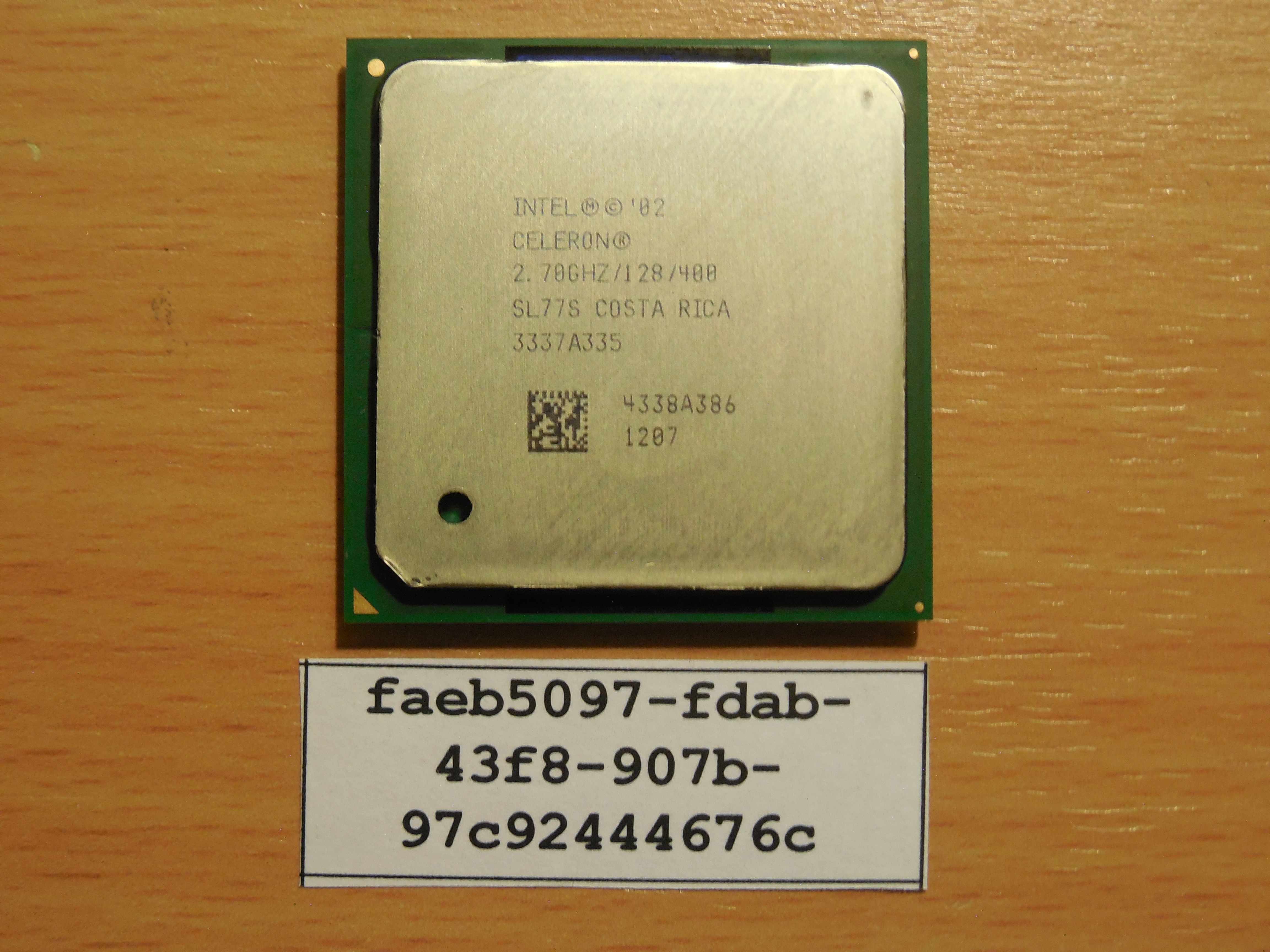
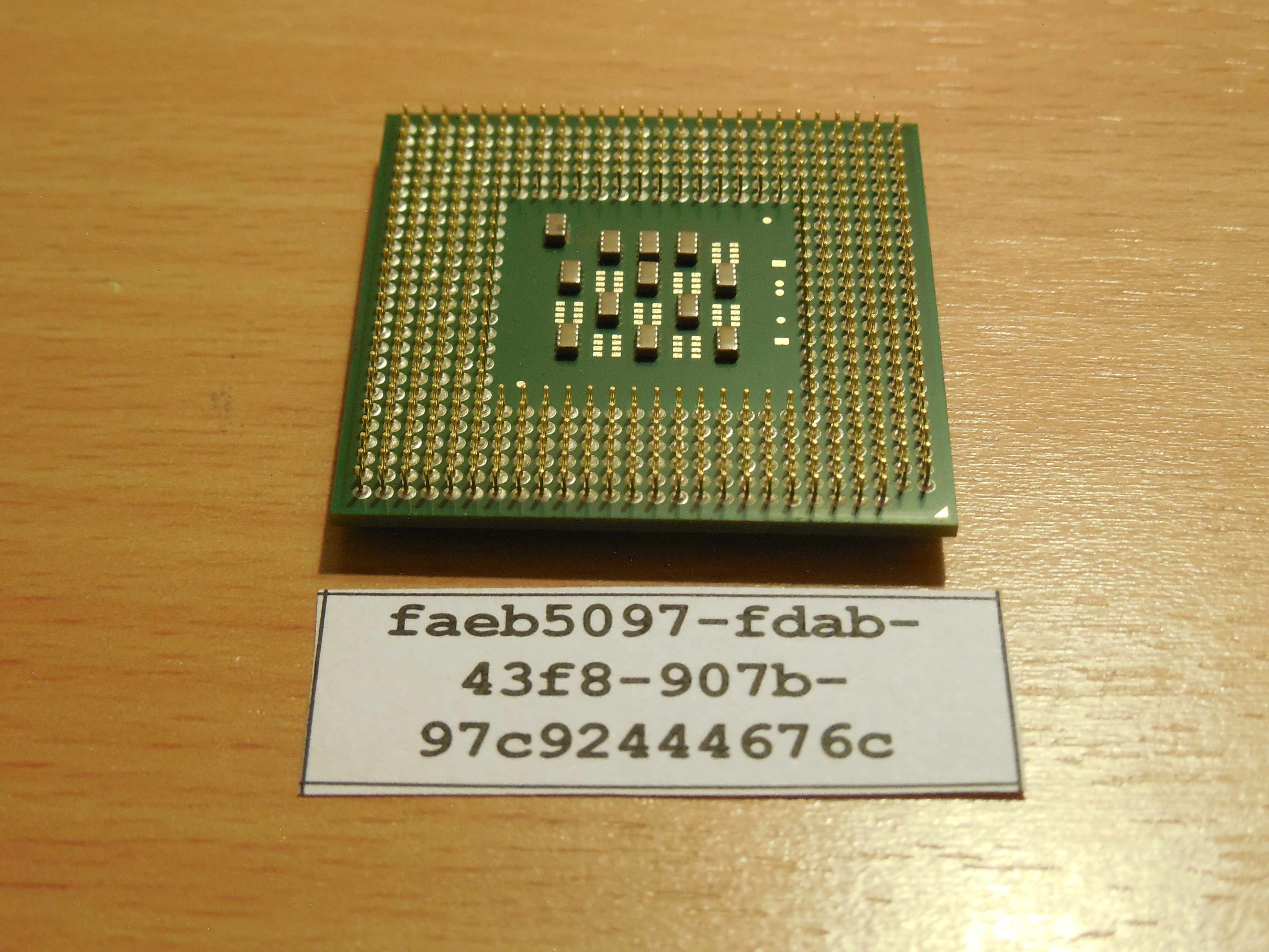
Процессор Intel Celeron SL77S Socket 478 2.7 GHz
SL77S specifications
| General information | |
| Type | CPU / Microprocessor |
| Family | Intel Celeron |
| Part number | BX80532RC2700B RK80532RC068128 |
| Frequency (GHz) ? | 2.7 |
| Bus speed (MHz) ? | 400 |
| Clock multiplier ? | 27 |
| Package type | 478-pin FC-PGA2 |
| Socket type | Socket 478 (mPGA478B) |
| Architecture / Microarchitecture / Other | |
| CPUID | 0F29h |
| Core stepping | D1 |
| Processor core | Northwood-128 |
| Manufacturing technology (micron) | 0.13 |
| Number of cores | 1 |
| L2 cache size (KB) ? | 128 |
| Core voltage (V) ? | 1.25 — 1.525 |
| Case temperature (°C) ? | 74 |
| Notes on sSpec SL77S | |
|
|
Related S-Spec numbers
In addition to the SL77S S-Spec, this processor was also manufactured with one production S-Spec number:
| Stepping | S-Spec | RK80532RC068128 | BX80532RC2700B |
|---|---|---|---|
| D1 | SL77S | + | + |
| SL77U | + |
SL77S CPUID information
| Intel Celeron 2.70 GHz SL77S | |||||||||
|---|---|---|---|---|---|---|---|---|---|
|
|
||||||||
| General information | |
|---|---|
| Vendor: | GenuineIntel |
| Processor name (BIOS): | Intel(R) Celeron(R) CPU 2.70GHz |
| Logical processors: | 1 |
| Processor type: | Original OEM Processor |
| CPUID signature: | F29 |
| Family: | 15 (0Fh) |
| Model: | 2 (02h) |
| Stepping: | 9 (09h) |
| TLB/Cache details: | Data TLB: 4-KB or 4-MB pages, fully associative, 64 entries Instruction TLB: 4-KB, 2-MB or 4-MB pages, fully associative, 128 entries No 2nd-level cache or, if processor contains a valid 2nd-level cache, no 3rd-level cache |
| Cache: | L1 data | L1 instruction | L2 |
|---|---|---|---|
| Size: | 8 KB | 12K uops | 128 KB |
| Associativity: | 4-way set associative |
8-way set associative |
2-way set associative |
| Line size: | 64 bytes | 64 bytes | |
| Comments: | sectored cache | sectored cache |
| Instruction set extensions | Additional instructions | ||
|---|---|---|---|
| MMX | CLFLUSH | ||
| SSE | CMOV | ||
| SSE2 | CMPXCHG8B | ||
| FXSAVE/FXRSTORE | |||
| SYSENTER/SYSEXIT | |||
| Major features | Other features | ||
| On-chip Floating Point Unit | 36-bit page-size extensions | ||
| Advanced programmable interrupt controller | |||
| Debug store | |||
| Debugging extensions | |||
| L1 context ID | |||
| Machine check architecture | |||
| Machine check exception | |||
| Memory-type range registers | |||
| Model-specific registers | |||
| Page attribute table | |||
| Page global extension | |||
| Page-size extensions (4MB pages) | |||
| Pending break enable | |||
| Physical address extensions | |||
| Self-snoop | |||
| Thermal monitor | |||
| Thermal monitor and software controlled clock facilities | |||
| Time stamp counter | |||
| Virtual 8086-mode enhancements | |||
| xTPR Update Control | |||
Процессор Intel Pentium E2140 SLA3J Socket LGA775

SLA3J specifications
General information
Type CPU / Microprocessor
Family Intel Pentium Dual-Core
Processor number ? E2140
Part number HH80557PG0251M
BX80557E2140
BXC80557E2140
Frequency (GHz) ? 1.6
Bus speed (MHz) ? 800
Clock multiplier ? 8
Package type 775-land FC-LGA6
Socket type Socket 775 (LGA775)
Architecture / Microarchitecture / Other
CPUID 06F2h
Core stepping L2
Next stepping QYRG
Next production stepping SLA93
Processor core Allendale
Manufacturing technology (micron) 0.065
Number of cores 2
L2 cache size (MB) ? 1
Features EM64T technology ?
Enhanced SpeedStep technology ?
Execute disable bit ?
Extended Halt state
Thermal Monitor 2
Core voltage (V) ? 1.162 — 1.312
Case temperature (°C) ? 61.4
Thermal Design Power (Watt) ? 65
Notes on sSpec SLA3J
The processor supports the 775_VR_CONFIG_06 guidelines for processors with TDP up to 65 Watt, and Iccmax up to 75A.
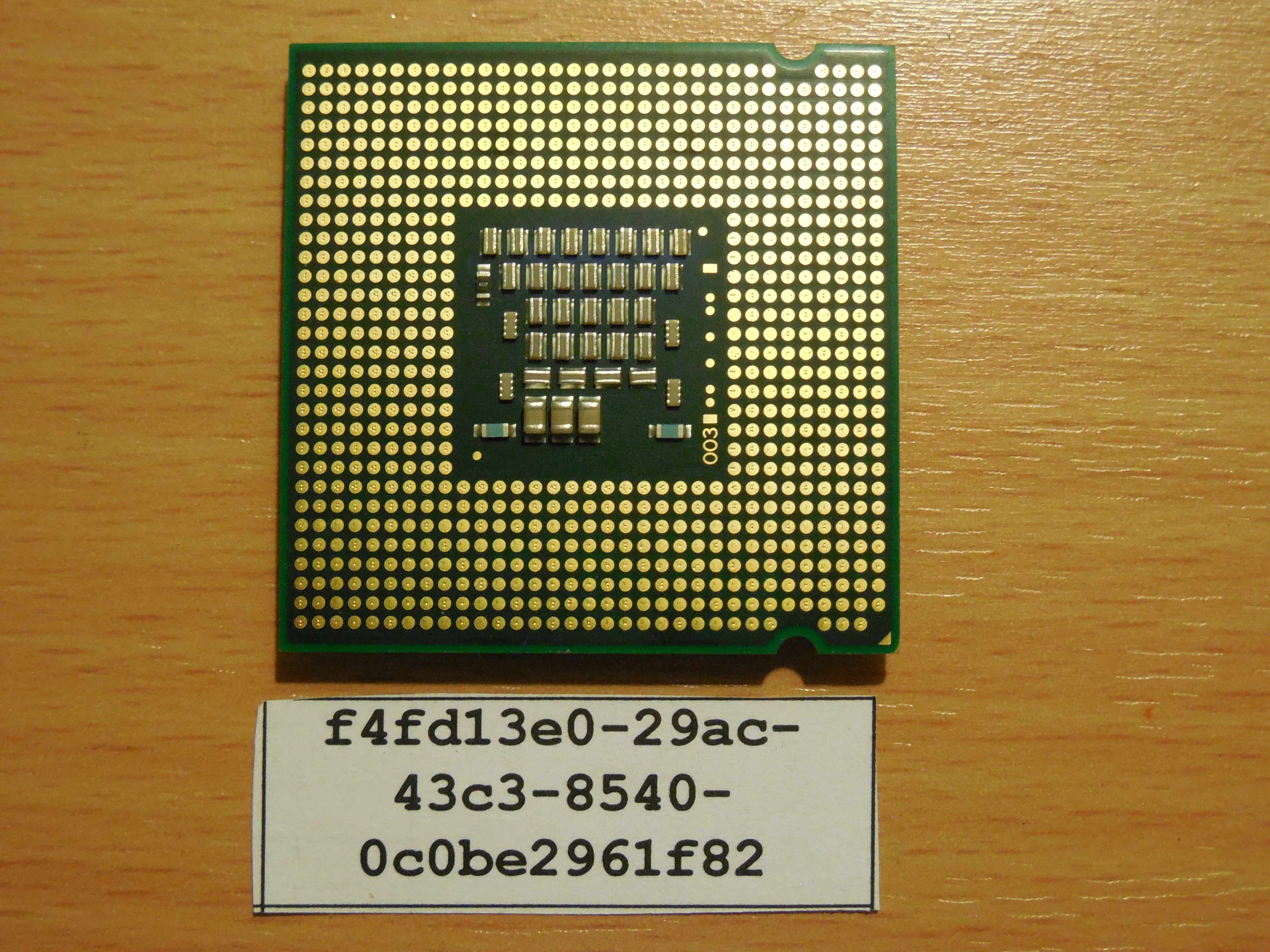
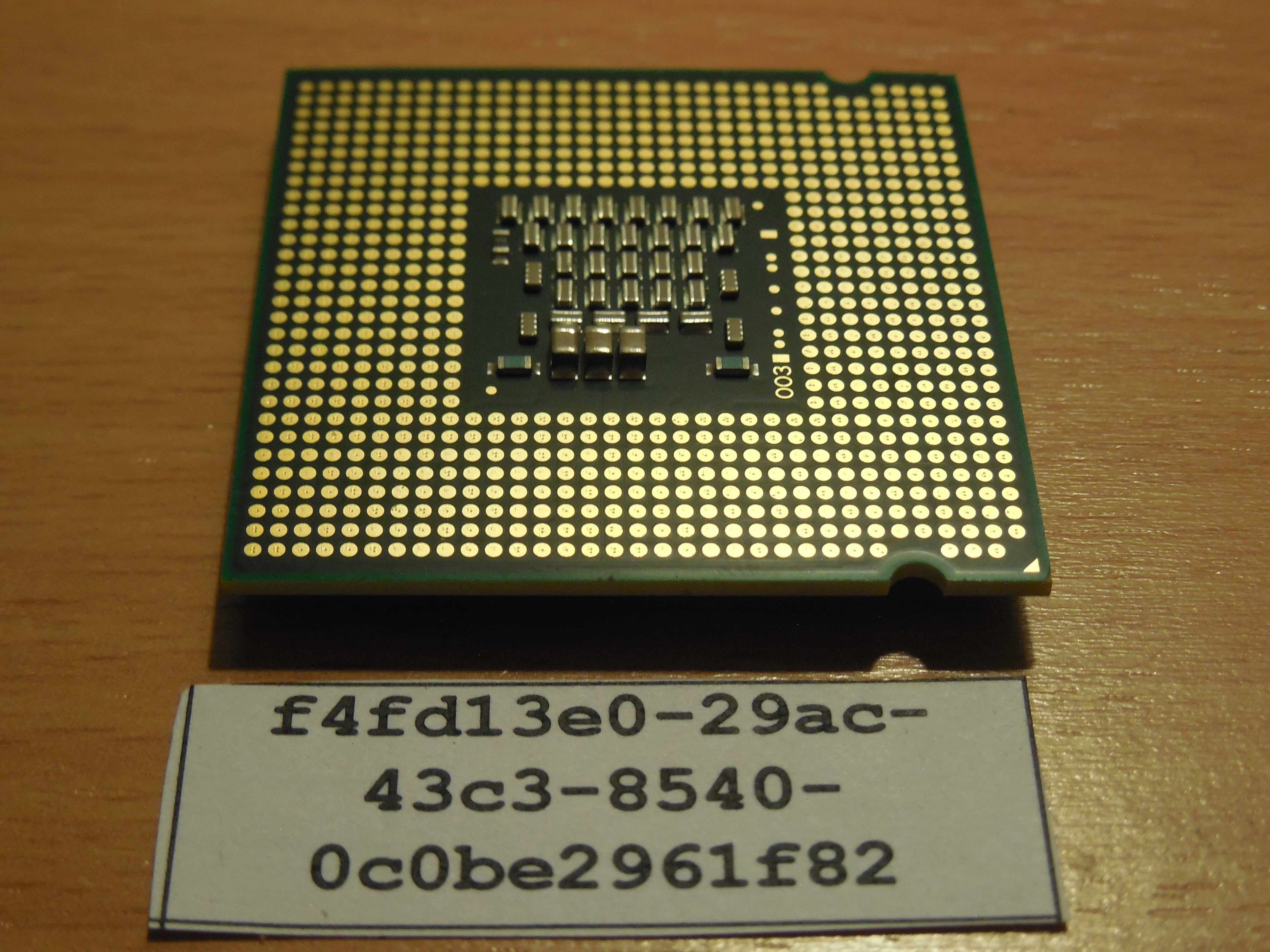
Процессор Intel Pentium 4 530J Socket LGA775 (SL7PU)
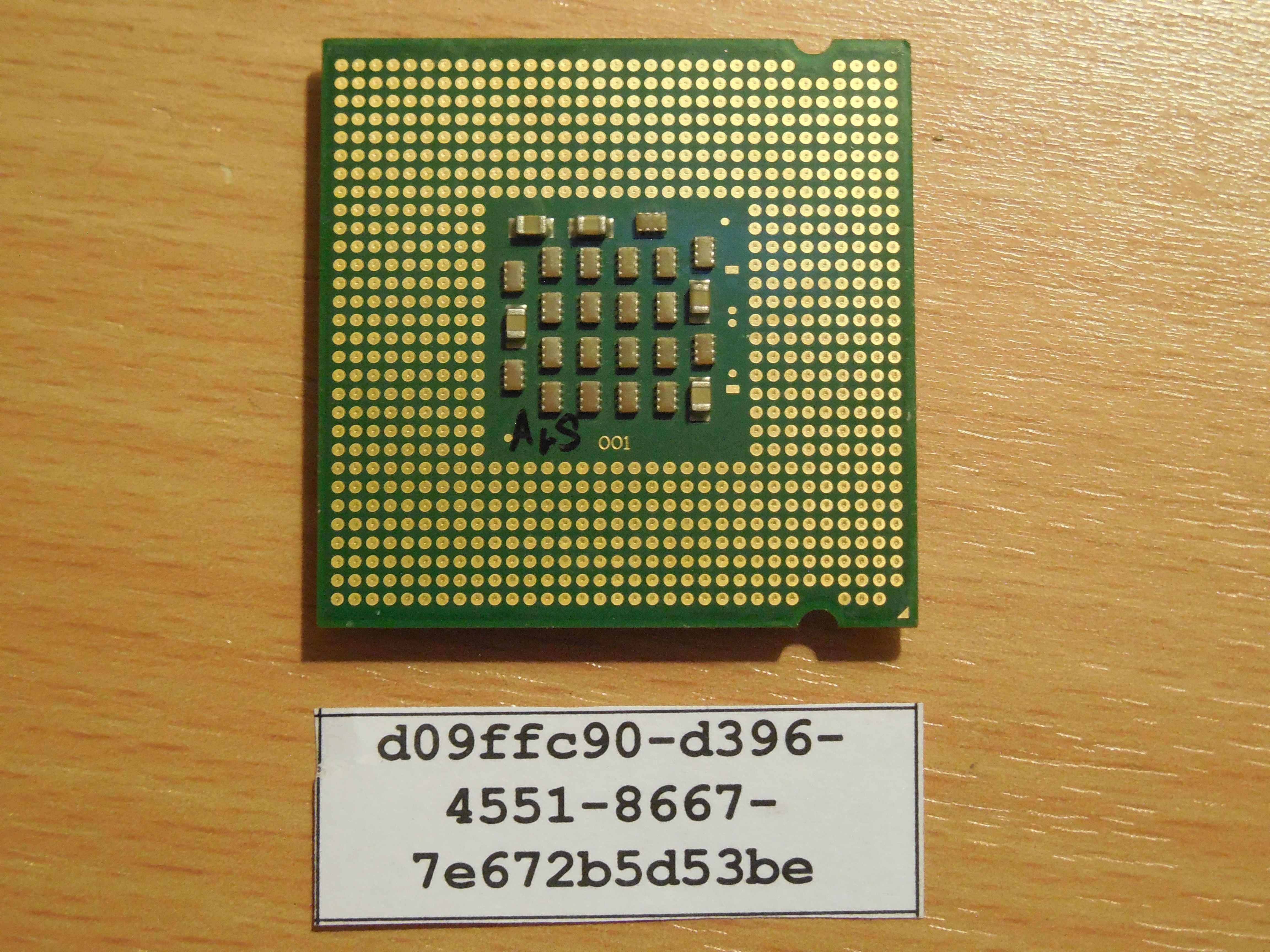
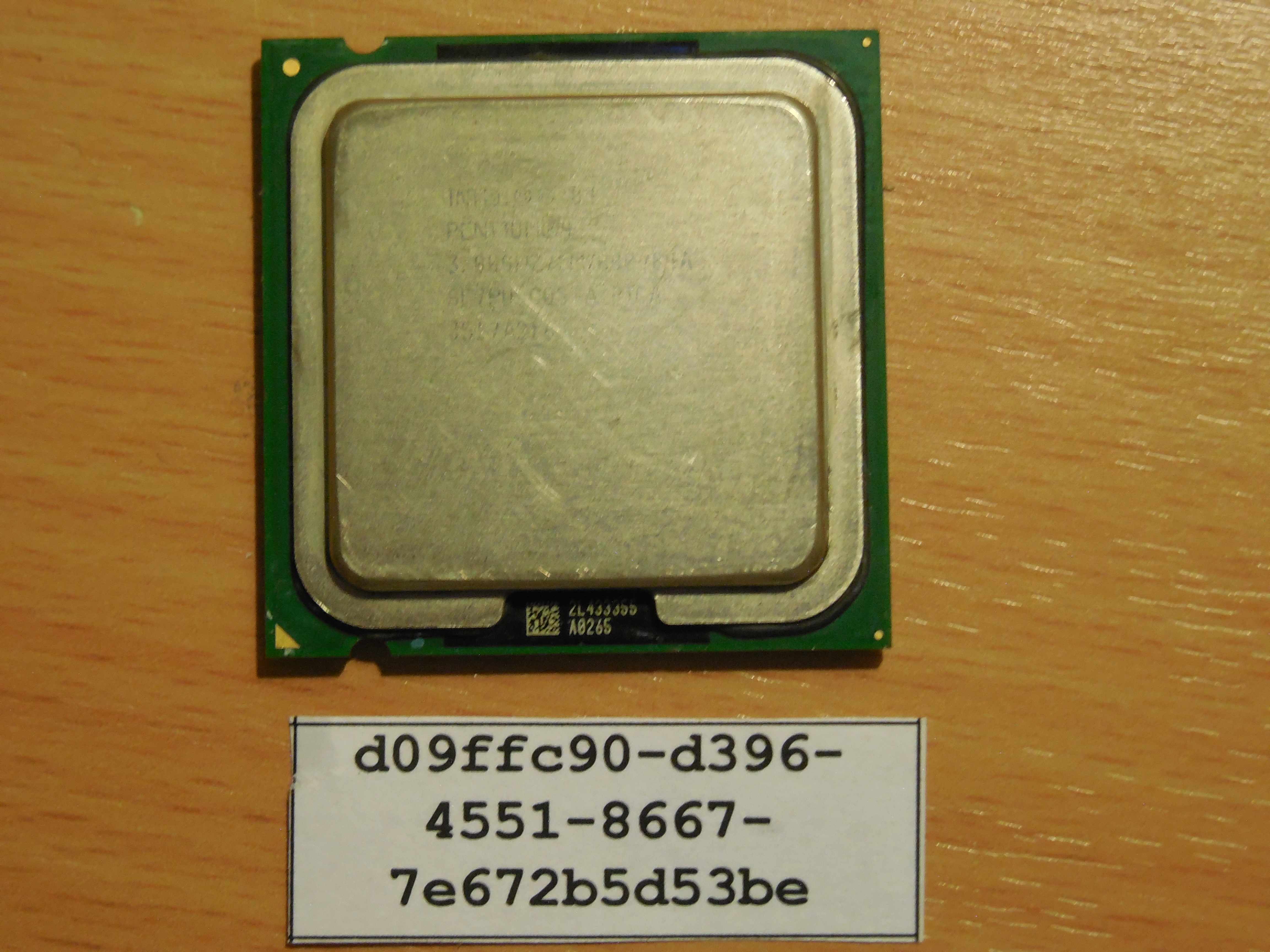
SL7PU specifications
General information
Type CPU / Microprocessor
Family Intel Pentium 4
Processor number ? 530J
Part number JM80547PG0801M
BX80547PG3000EJ
BX80547PG3000ET
Frequency (GHz) ? 3
Bus speed (MHz) ? 800
Clock multiplier ? 15
Package type 775-land FC-LGA4
Socket type Socket 775 (LGA775)
Architecture / Microarchitecture / Other
CPUID 0F41h
Core stepping E0
Qualification sample Q09X
Previous stepping SL7J6
Processor core Prescott
Manufacturing technology (micron) 0.09
L2 cache size (MB) ? 1
Features Execute disable bit ?
Hyper-Threading technology
Core voltage (V) ? 1.287 — 1.4
Case temperature (°C) ? 67.7
Notes on sSpec SL7PU
This part also ships as a boxed processor with an unattached fan heatsink.
Microprocessors with this S-Spec have multiple VIDs.
This S-spec supports the 775_VR_CONFIG_04A (mainstream) guidelines for processors with Iccmax up to 78A, and VID up to 1.4V.
This part has Enhanced Halt State enabled.
The parts are available starting from October 1, 2004
Changes in E0 stepping: Execute disable bit, additional power management features.
Процессор AMD Athlon 64 ADA3000AEP4AR Socket 754 3000+
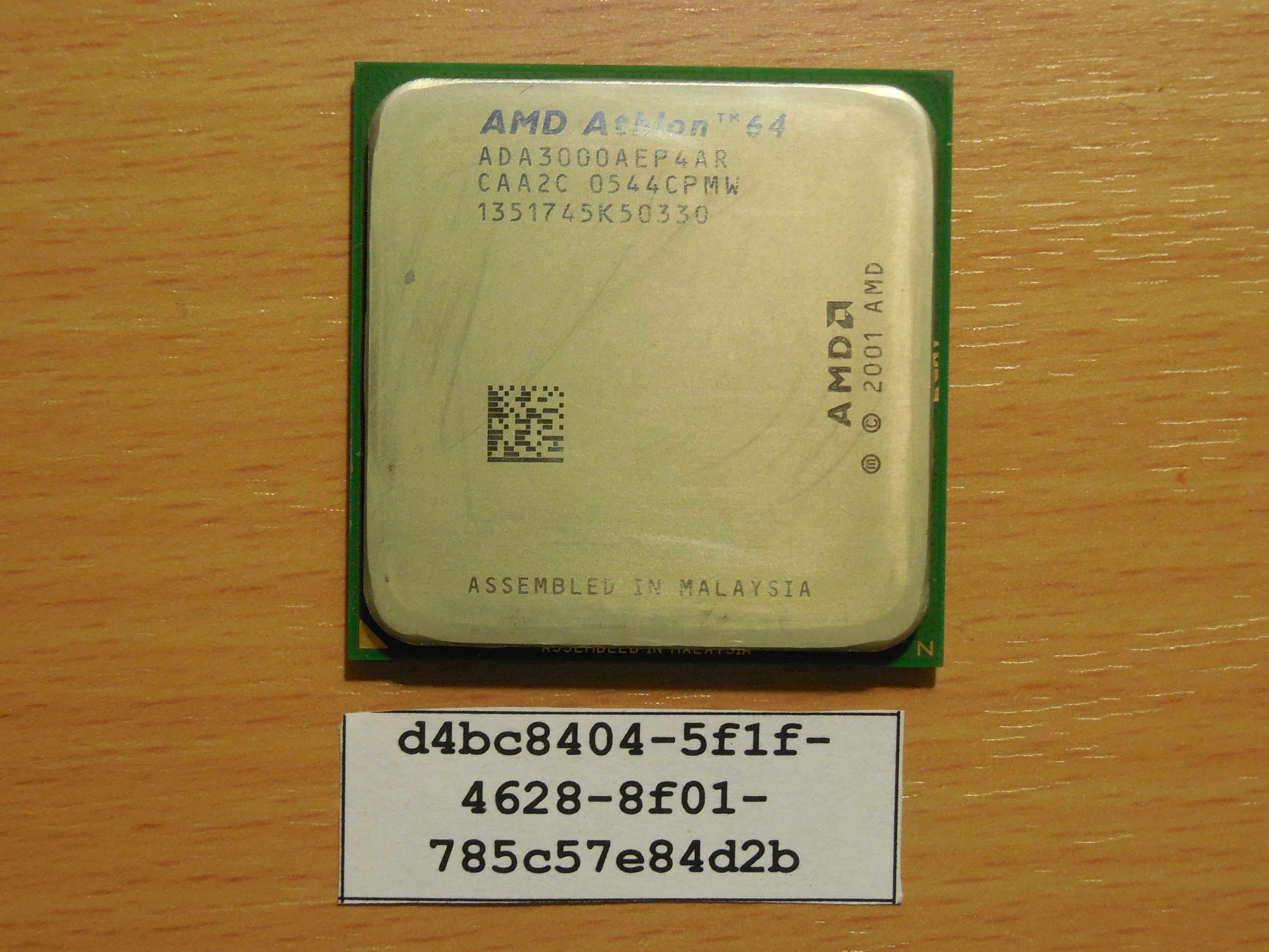

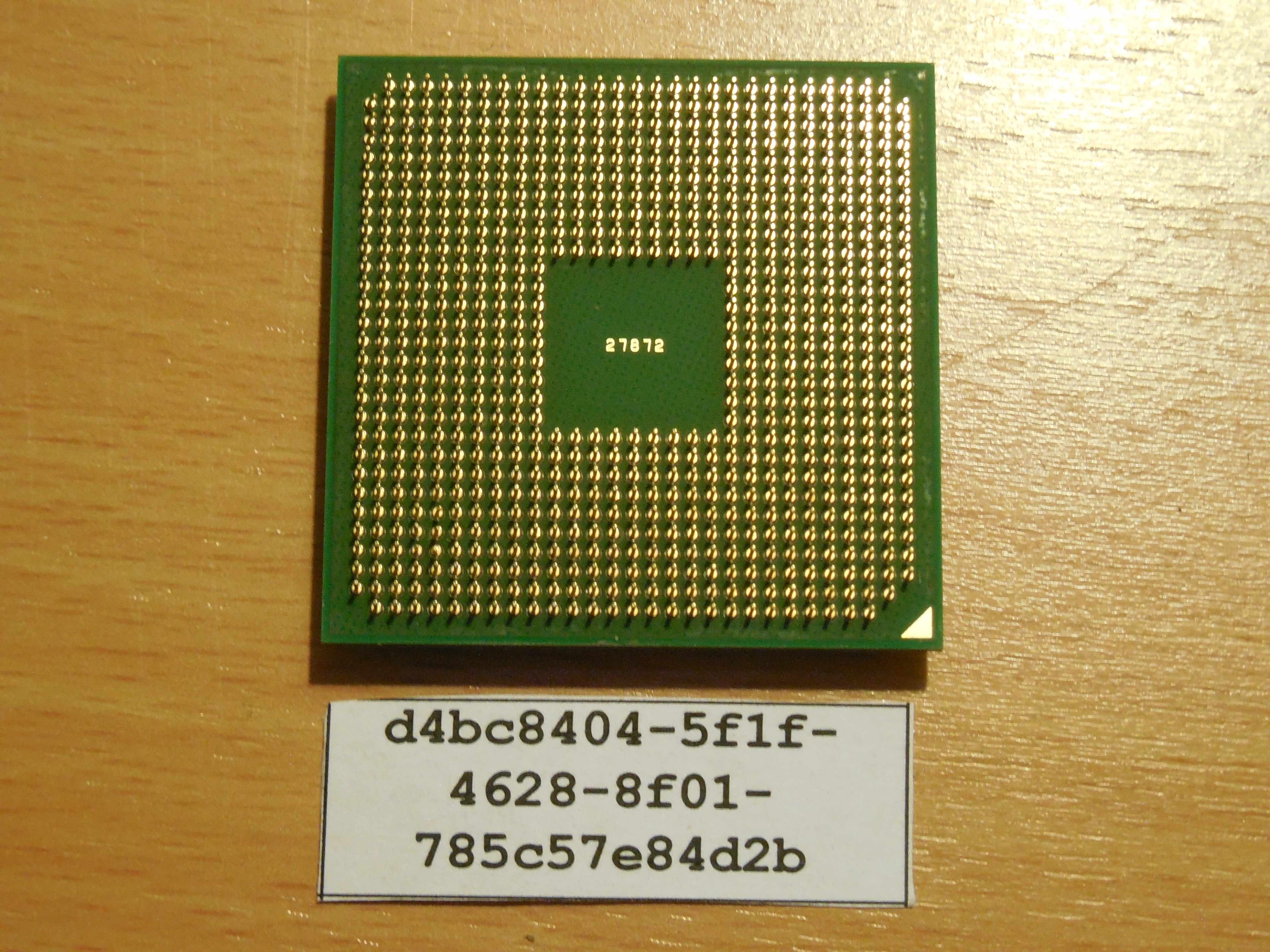
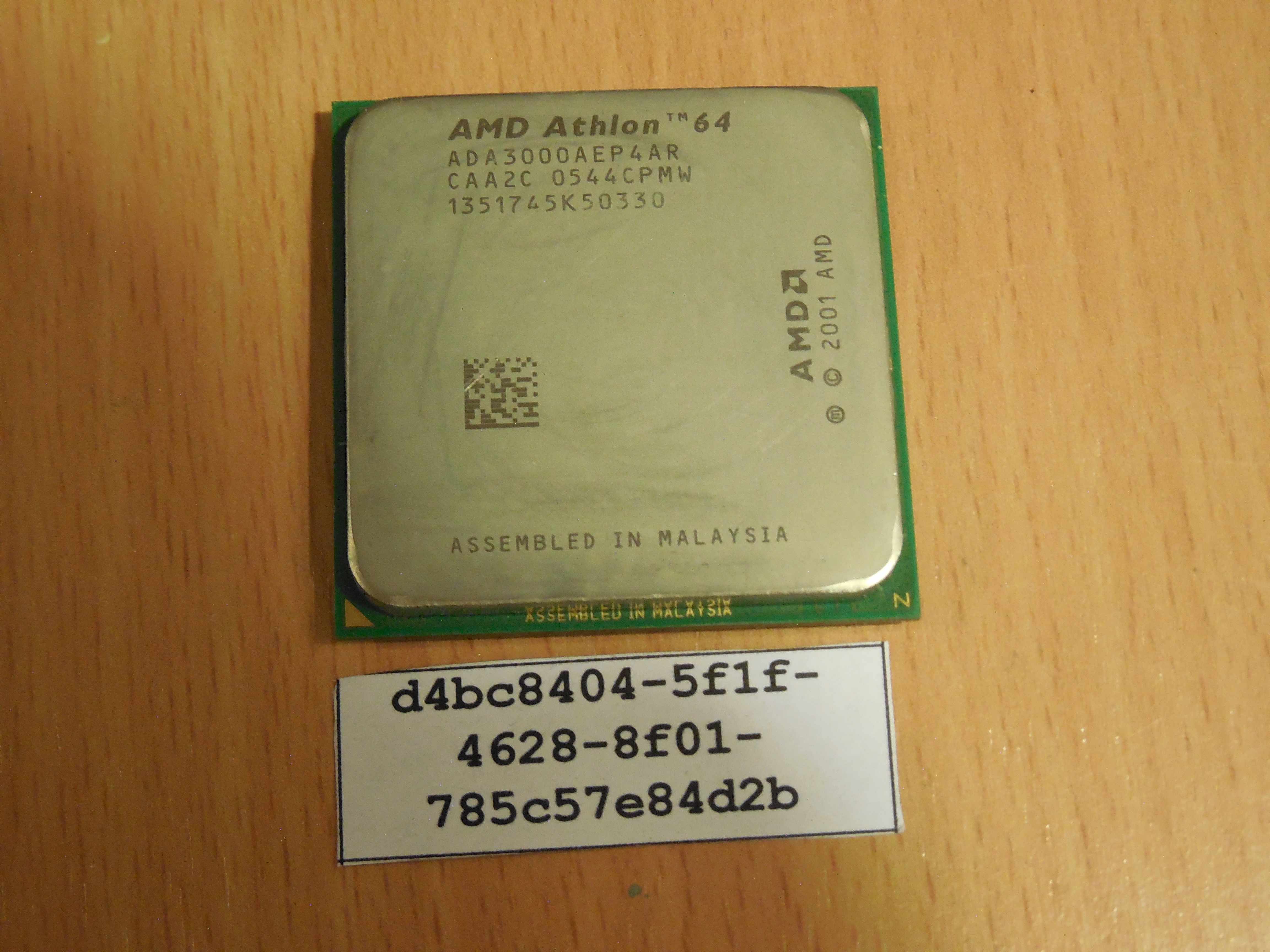
General information
Type CPU / Microprocessor
Market segment Desktop
Family AMD Athlon 64
Model number ? 3000+
CPU part numbers
ADA3000AEP4AR is an OEM/tray microprocessor
ADA3000BOX is a boxed microprocessor
Stepping codes AAARC CAA2C CAAPC CAAZC
Frequency ? 3000+ (rated)
2000 MHz (real)
Clock multiplier ? 10
Package 754-pin lidded microPGA
1.57″ x 1.57″ (4 cm x 4 cm)
AMD Package number 27872
Socket Socket 754
Architecture / Microarchitecture
Microarchitecture K8
Processor core ? ClawHammer
Core stepping ? SH-CG
CPUID F4A
Manufacturing process 0.13 micron silicon-on-insulator (SOI) technology
Data width 64 bit
The number of cores 1
The number of threads 1
Floating Point Unit Integrated
Level 1 cache size ? 64 KB 2-way set associative instruction cache
64 KB 2-way set associative data cache
Level 2 cache size ? 512 KB exclusive 16-way set associative cache
Physical memory 1 TB
Virtual memory 256 TB
Multiprocessing Uniprocessor
Features
MMX instructions
Extensions to MMX
3DNow! technology
Extensions to 3DNow!
SSE / Streaming SIMD Extensions
SSE2 / Streaming SIMD Extensions 2
AMD64 / AMD 64-bit technology ?
EVP / Enhanced Virus Protection ?
Low power features
Halt state
Stop Grant state ?
Cool’n’Quiet technology
Integrated peripherals / components
Integrated graphics None
Memory controller The number of controllers: 1
Memory channels: 1
Supported memory: DDR
Other peripherals One 16-bit HyperTransport link with speeds up to 800 MHz
Electrical / Thermal parameters
V core ? 1.5V
Maximum operating temperature ? 70°C
Thermal Design Power ? 89 Watt
Notes on AMD Athlon 64 3000+
In the minimum performance state (P-state) the processor runs at 1000 MHz and 1.1 Volt core voltage. Thermal Design Power in the minimum P-state is 22 Watt
[ПРОДАНО] Процессор Intel Pentium II 400 MHz (SL357) с кулером и радиатором

400/512/100/2.0V S1
19380582R-0234 Philippines
imc ’97 SL357
Процессор Intel® Celeron® SL6C7 Socket 370 1.30 GHz, 256K Cache, 100 MHz FSB


Specifications
—
Essentials
Status End of Interactive Support
L2 Cache 256 KB
FSB Speed 100 MHz
FSB Parity No
Instruction Set 32-bit
Embedded Options Available No
Lithography 130 nm
VID Voltage Range 1.5V
Recommended Customer Price N/A
Datasheet Link
—
Performance
# of Cores 1
Processor Base Frequency 1.3 GHz
TDP 33.4 W
—
Memory Specifications
Physical Address Extensions 32-bit
ECC Memory Supported No
—
Package Specifications
TCASE 71°C
Package Size 49mm x 49mm
Processing Die Size 80 mm2
# of Processing Die Transistors 44 million
Sockets Supported PPGA370
Low Halogen Options Available See MDDS
—
Advanced Technologies
Intel® Turbo Boost Technology No
Intel® Hyper-Threading Technology No
Intel® Virtualization Technology (VT-x) No
Intel® 64 No
Idle States No
Enhanced Intel SpeedStep® Technology No
Intel® Demand Based Switching No
—
Intel® Platform Protection Technology
Trusted Execution Technology No
Execute Disable Bit No